Lab 6 - ECE 421L
Author: Nicholas Mingura
Email: mingura@unlv.nevada.edu
Prelab:
For the Prelab the students were tasked at making a NAND gate with two inputs from tutorial 4.

Image 1: NAND gate Schematic
After making the schematic view the layour was created with no DRC errors and with the LVS net lists matching
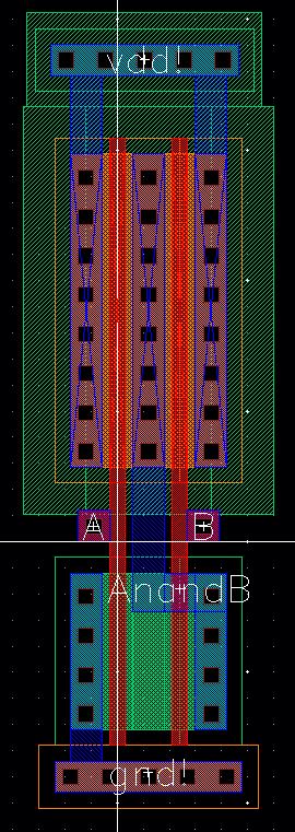
Image 2: NAND gate Layout
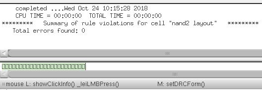
Image 3:NAND gate DRC
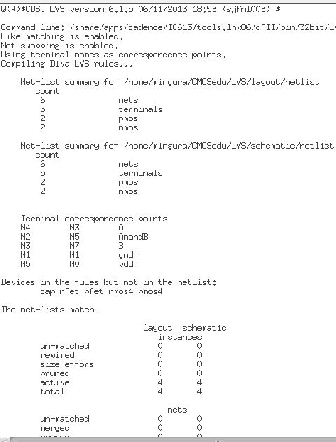
Image 4:NAND gate LVS
To ensure that the NAND gate was working correctly simulations were done showing that the truth table held true.
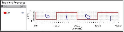
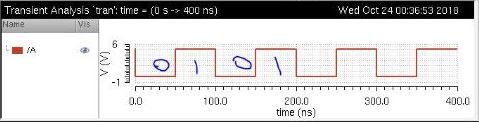
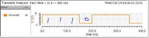
Image 5: NAND gate simulation
Lab:
For the lab the first task was to create a xor gate using the schematic image that was provided in the lab description
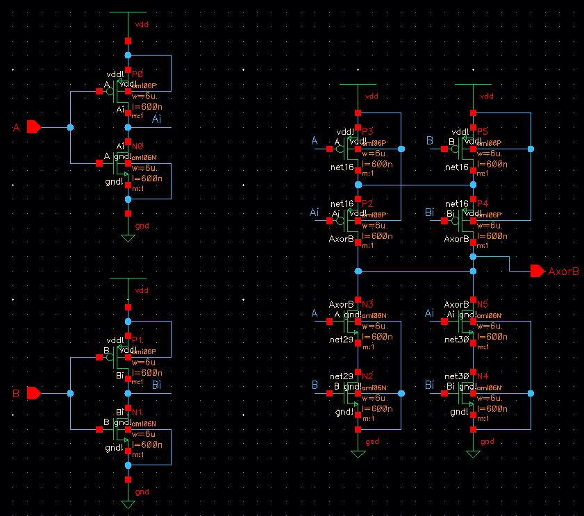
Image 6: Xor Schematic
After making the schematic the next step was to create a symobl for the XOR gate with our name and semester we built it in.
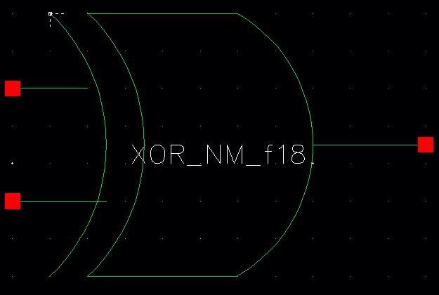
Image 7: XOR gate symbol
Following the symbol the layout was made with no DRC errors, and with the LVS netlists matching.
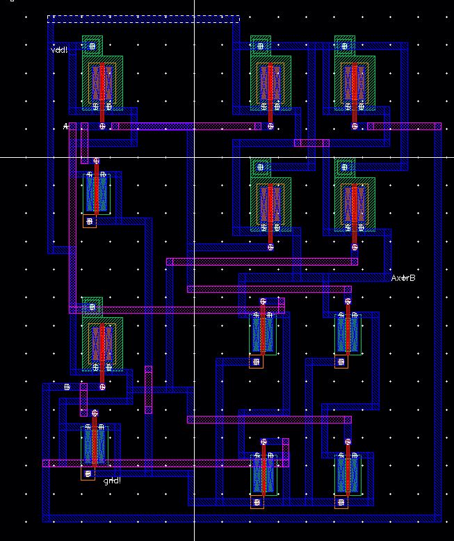
Image 8:XOR Layout view
file:///C:/Users/oit/Desktop/Lab_6/Full_Adder_Schematic.JPG

Image 9:XOR DRC

Image 10:XOR LVS
After
making sure that the netlists match an A and B input were given to the
XOR gate to test the output of the XOR to ensure that it was working
correctly.
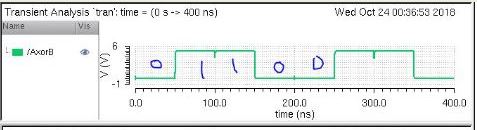
Image 11:XOR Simulation inputs and outputs.
Now that all of the gate components were made the following step was to make the full adder schematic.
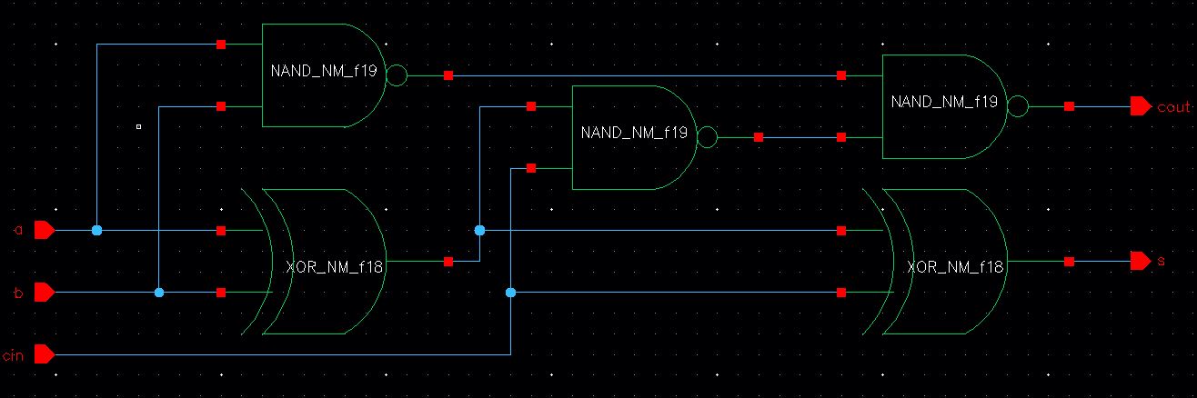
Image 11:Full Adder Schematic
After the schematic was made the Layout view was constructed with no DRC errors and with the LVS netlist matching.
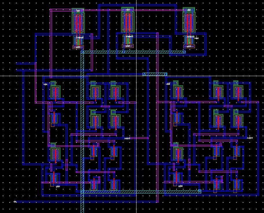
Image 12:Full Adder Layout view
Image 13:Full Adder DRC
Image 14:Full Adder LVS
Return to Nicholas Mingura's Labs
Return to EE 421L Students
Return to EE 421L Home